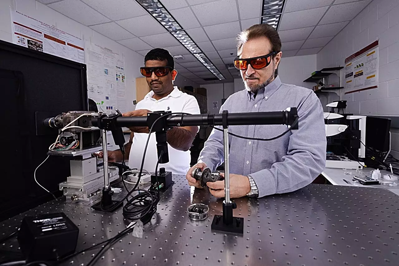
In 1999, Valery Levitas embarked on a transformative journey from Europe to the United States, bringing along his pioneering rotational diamond anvil cell. This sophisticated tool has since evolved, retaining its core function of squeezing and shearing materials between diamond surfaces. It allows researchers to observe the intricate processes at play during material deformation and verify theoretical predictions in real-time. Among the questions this research tackles are critical inquiries such as: How do the structures of crystals morph under stress? What new qualities can emerge from these alterations? And how does the application of shearing influence the levels of pressure required to engender new material phases?
Levitas, an esteemed professor at Iowa State University, emphasizes the interdisciplinary nature of their research, which resides at the crossroads of mechanics, physics, material science, and applied mathematics. In a recent study published in Nature Communications, Levitas and his team unveiled intriguing findings regarding silicon, a material fundamental to modern electronics. Their research illustrates that silicon undergoes unexpected phase transformations when subjected to significant pressures coupled with plastic, or permanent, deformation.
Unlike previous studies that focused solely on silicon’s response to high pressures, this research delves into the synergies between pressure and plastic strain. The experimental setup utilized different particle sizes of silicon—specific dimensions at the nanoscale—to explore how these alterations manifest. The findings reveal that under room-temperature conditions, silicon particles measuring 100 billionths of a meter can transition from their “Si-I” phase to the “Si-II” phase at a mere 0.3 gigapascals, a remarkable contrast to the previously established threshold of 16.2 gigapascals for high-pressure-only transitions.
Levitas describes this significant reduction in necessary transformation pressure as groundbreaking. The utility of enhancing phase transformations through plastic deformation at such low pressures holds promising implications for various industrial applications. The challenge, as Levitas articulates, has been to explore this less frequented research terrain of low-pressure transformations while maintaining the integrity of material structures. It is not merely about altering the size and shape of the samples; rather, it is about instigating changes in the microstructure that lead to beneficial phase transformations.
The research team examined seven distinct phases of silicon, each associated with unique lattice structures that confer varying properties advantageous for real-world applications. This novel approach offers the tantalizing possibility of tailoring nanostructured pure phases or composites to achieve optimized electrical, optical, and mechanical characteristics.
A significant hurdle in material sciences has been the impracticality of utilizing very high pressures in industrial settings. Levitas suggests that the application of plastic deformations presents a more feasible pathway for industries to access the desirable high-pressure phases and their attendant properties, all while working at substantially lower pressures. This breakthrough could have far-reaching implications in fields such as electronics and materials manufacturing, where the ability to modify material properties reliably and economically is paramount.
Reflecting on his two-decade-long scientific inquiries, Levitas expresses that he always anticipated silicon’s uncommon response to the unique strains exerted by the rotational diamond anvil cell. This foresight only propelled his team to investigate further. The research not only signifies a substantial advancement in our understanding of silicon’s behaviors but also paves the way for future studies aimed at harnessing these findings for practical applications.
A New Front in Material Science
As the research progresses, the collaboration of experienced scientists like Sorb Yesudhas, and institutions such as Argonne National Laboratory, augments the fabric of this exploration into complex material behaviors. With an upsurge in possibilities for practical implementations, Levitas and his team’s groundbreaking work signals an exciting new front in material science, urging industry stakeholders to reconsider traditional boundaries of material experimentation and usage. The implications of their findings may well inspire a wave of innovations in electronics and beyond, fundamentally reshaping how industries approach material synthesis and application for generations to come.


Leave a Reply