
In the pursuit of miniaturized optoelectronic devices, researchers have turned their attention to two-dimensional (2D) superconducting materials. These materials hold promise for creating smaller devices that perform efficiently while consuming less energy. One key requirement for these devices is a higher gate capacitance to store more electrical charge in relation to the voltage applied, without compromising the thickness of gate insulators or gate dielectrics. This has led researchers to explore the use of insulating materials with a high dielectric constant (κ), such as hafnium oxide (HfO2).
While high-κ materials like hafnium oxide offer a potential solution, they have proven difficult to integrate with 2D semiconductors in the past. This challenge has prompted researchers at Fudan University to explore new avenues. They have recently developed a 2D perovskite oxide with a high dielectric constant that can be successfully integrated with a variety of 2D channel materials. This groundbreaking research, published in Nature Electronics, opens up new possibilities for downscaled optoelectronic devices.
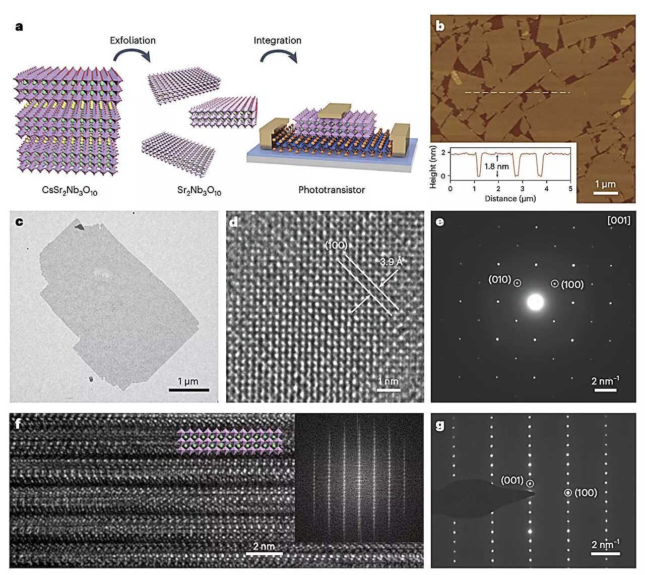
The Synthesis of Sr2Nb3O10: A Game-Changer in Optoelectronics
The 2D perovskite oxide, Sr2Nb3O10, introduced in the researchers’ paper, was synthesized through a top-down preparation strategy. This approach allowed them to create SNO nanosheets, which could then be transferred onto different 2D materials. Sr2Nb3O10 boasts a high dielectric constant of 24.6 and a moderate bandgap, making it an ideal photoactive high-κ dielectric for phototransistors based on various 2D semiconducting materials like graphene, molybdenum disulfide, tungsten disulfide, and tungsten diselenide.
Performance Evaluation: Integrating Sr2Nb3O10 with Channel Materials
To assess the potential of Sr2Nb3O10 in developing miniaturized optoelectronics, the researchers conducted tests by transferring it onto different channel materials, including molybdenum disulfide and tungsten disulfide. The results were promising, with molybdenum disulfide transistors showcasing an impressive on/off ratio and subthreshold swing. Similarly, tungsten disulfide phototransistors exhibited a high photocurrent-to-dark-current ratio and UV responsivity under visible or UV light illumination.
The study’s findings revealed the successful integration of Sr2Nb3O10 with various channel materials through a straightforward procedure. The researchers highlighted the establishment of a well-defined interface between the semiconductor and dielectric, along with the high dielectric constant of Sr2Nb3O10, enabling efficient gate control of channel materials. Additionally, the phototransistors incorporating the photoactive dielectric demonstrated dual-band photodetection capabilities for UV and visible light illumination.
Future Implications
The groundbreaking work by Siyuan Li, Xinya Liu, and their team paves the way for the synthesis of additional 2D perovskite oxides that can be seamlessly integrated with existing semiconductors and channel materials. These advancements hold the potential to revolutionize the field of electronics and optoelectronics, leading to the development of smaller, more efficient, and energy-saving devices in the near future.
Leave a Reply