
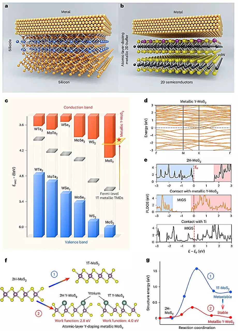
Electronics engineers and materials scientists have been tirelessly seeking out materials that can enhance the performance of electronics beyond the capabilities of silicon-based transistors. One promising solution that has emerged is the use of two-dimensional (2D) semiconductors. These materials offer unique properties that make them ideal candidates for the improvement of transistor performance. Notably, 2D semiconductors are incredibly thin at an atomic level and demonstrate high carrier mobilities, which could lead to more effective electrostatic control and enhanced ON-state performances in field-effect transistors (FETs). However, despite these advantages, 2D semiconductors have been plagued by high contact resistances caused by Fermi-level-pinning effects, which have severely hindered their performance in transistors.
A recent study conducted by researchers at Peking University and Chinese Academy of Sciences has introduced a novel yttrium-doping strategy that aims to address the critical limitation of 2D semiconductors. This new approach could potentially pave the way for the seamless integration of 2D semiconductors in electronic devices. By converting semiconducting molybdenum disulfide (MoS2) into metallic MoS2 through yttrium doping, researchers have been able to enhance band alignment and enable the fabrication of ohmic contacts for 2D transistors. The key to this strategy lies in the insertion of a semi-metal layer between a metal electrode and a two-dimensional semiconductor, improving carrier injection efficiency and drawing inspiration from the structure of silicide in silicon-based transistors.
The research team devised a plasma-deposition-annealing (PDA) method to carry out yttrium doping on the surface layer of MoS2. This innovative technique involved treating patterned local contact areas with low-power soft plasma to create active sites. Subsequently, a Y/Ti/Au stacked metal was deposited, with a 1 nm-thick active metal Y serving as a solid-state doping source. Yttrium atoms diffused into the active sites and were activated in the top layer of the material through high-temperature annealing in an inert gas environment. The PDA doping process demonstrated exceptional thermal stability after annealing, making it compatible with advanced-node wafer-scale integration.
The study also introduced a groundbreaking concept known as “rare earth element yttrium doping-induced 2D phase transition.” This phase transition essentially refers to the metallization that occurs when the yttrium doping strategy is applied to MoS2. The researchers successfully developed ultra-short MoS2-based channel ballistic transistors with exceptional performance as ohmic contacts, boasting impressive switching capabilities. Looking ahead, these transistors have the potential to usher in a new era of sub-1 nanometer node chips that offer unparalleled performance while consuming minimal power compared to traditional chips.
Moving forward, the researchers are focused on enhancing their yttrium-doping strategy to create equally superior p-type ohmic contacts suitable for 2D semiconductors. With continued innovation in materials science and engineering, the possibilities for revolutionizing electronic devices are limitless. The integration of 2D semiconductors into electronics could lead to monumental advancements in the field, offering faster, more efficient, and energy-saving devices for a multitude of applications. By overcoming the limitations of silicon-based transistors through innovative approaches like yttrium doping, we are on the brink of a new era in electronics.
Leave a Reply