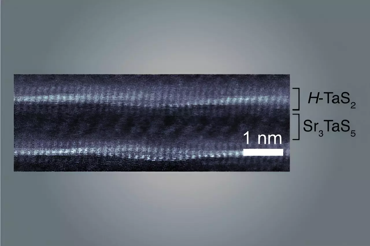
In an impressive feat of scientific ingenuity, physicists from the Massachusetts Institute of Technology (MIT) have synthesized a groundbreaking material that exhibits remarkable superconducting and metallic properties. This material stands out not only due to its unique characteristics but also because of its macroscopic size, allowing for tangible manipulation and observation. The innovation hinges on wavy atomic structures, compact yet intricate, that span layers a billionth of a meter thick. This discovery, published in the esteemed journal *Nature*, revolutionizes how researchers perceive and interact with the quantum behaviors of materials.
One of the most significant aspects of this research lies in the method of synthesis, which relies on rational design. The scientists did not stumble upon this material by chance; rather, they meticulously crafted it based on thorough insights into materials science. With a deep understanding of the chemistry involved in this family of materials, the MIT team is confident that they can engineer even more new materials characterized by unusual properties. This approach is a step forward in materials science, shifting the narrative from serendipitous discovery to intentional and controlled fabrication.
The newly developed material consists of repeating layers that create a wave-like atomic architecture, a phenomenon that, according to the researchers, has not been perfected in prior materials. The crystal is formed by thousands of these wavy layers, each comprising a thin metallic layer of tantalum and sulfur placed above a spacer layer composed of strontium, tantalum, and sulfur. This layered design emerges from a size and structural mismatch within the crystal lattice, leading to a buckling effect reminiscent of a larger sheet of paper compressing on a smaller one.
Such uniformity across the entire crystal is vital, as it allows for consistent properties when studying the material’s behavior and performance. Joseph Checkelsky, one of the senior investigators of the study, highlights this opportunity to delve deeper into physical properties that extend beyond conventional crystal systems, stating that understanding these new characteristics represents a significant frontier in materials research.
At the heart of the new material’s appeal is its superconducting property, where electrons can traverse the material without resistance, a critical feature for future electronic technologies. The structure of the material imprints a wave pattern onto the flow of electrons, causing variations in superconductivity strength across different regions. These localized differences can result in novel functionalities, making the material an exciting candidate for applications across fields such as electronics and energy storage.
The material also exhibits unusual metallic characteristics, largely attributed to the topographical waves within its structure. Electrons find it significantly easier to flow down into the “troughs” of these waves rather than facing the obstacle of “hills.” This directional flow enhances performance and efficiency, allowing for better control of electrical conduction. According to Aravind Devarakonda, the first author of the research, this directionality introduced by the wave structure dramatically alters the behavior of the material, opening the door to new applications that could harness these exceptional properties.
Exploring Uncharted Territories in Materials Science
As researchers explore the vast landscape of materials beyond traditional frameworks, they are venturing into what Devarakonda describes as “uncharted territory.” This research significantly expands the existing repertoire of materials available for experimentation and application. The findings indicate that the integration of wavy structures into material design could yield unexpected outcomes—an exhilarating prospect that embodies the heart of scientific inquiry.
By leveraging insights gained from their studies, the researchers have laid a solid foundation for future exploration. The hope is that this material will catalyze a new wave of discoveries in the realm of superconductivity and other advanced properties. The collaborative efforts from various institutions, including contributions from students and esteemed researchers across disciplines, symbolize the collective pursuit of knowledge and innovation.
The development of this new superconducting material is more than just an academic achievement; it is a catalyst for future innovation in materials science. The ability to manipulate macroscopic samples with complex atomic structures could revolutionize electronic technologies, enhancing our understanding of quantum behaviors and potentially paving the way for new applications. As researchers continue to probe the capabilities and implications of their findings, the excitement surrounding this discovery emphasizes the transformative power of materials science in the modern world. Ultimately, this research heralds a promising future, where scientific curiosity and technological advancements converge to unravel the mysteries of the atomic world.


Leave a Reply