Recent advancements in semiconductor research have unveiled a groundbreaking technique that allows scientists to directly observe the behavior of electric charges as they traverse the interface between two distinct semiconductor materials. The study conducted by the UC Santa Barbara research team, led by associate professor Bolin Liao, offers unprecedented insights into the dynamic nature of charge carriers—an area that has previously relied heavily on theoretical models and indirect measurements. This work, published in the Proceedings of the National Academy of Sciences, marks a pivotal moment in semiconductor science, with implications for various technologies such as photovoltaics, lasers, and sensors.
At the heart of semiconductor functionality is the movement of electric charges, or photocarriers, which occur when a semiconductor material is exposed to light. This interaction excites electrons, causing them to generate a flow of electrical current. However, a critical issue arises with the energy dynamics of these photocarriers. They tend to lose a substantial portion of their energy within picoseconds, rendering traditional photovoltaic cells comparatively inefficient as they harness only a small fraction of the available energy during this transient “hot” state. Understanding the nuances of this process, especially how these carriers behave when crossing the heterojunction between different semiconductor materials, is essential for improving energy efficiency in electronic devices.
Heterojunctions—interfaces arising from the contact between two different semiconductor materials—play a crucial role in determining charge carrier dynamics. Properties such as laser performance and energy conversion efficiency in photovoltaics hinge on how effectively these carriers can transmit through these boundaries. As scientists strive to develop improved semiconductor devices, a comprehensive understanding of how photocarriers transfer at heterojunctions becomes indispensable. The collaboration between UCSB and UCLA facilitated the creation of a silicon-germanium heterojunction specifically for this research, showcasing the potential of widely-used semiconductor materials in next-generation technologies.
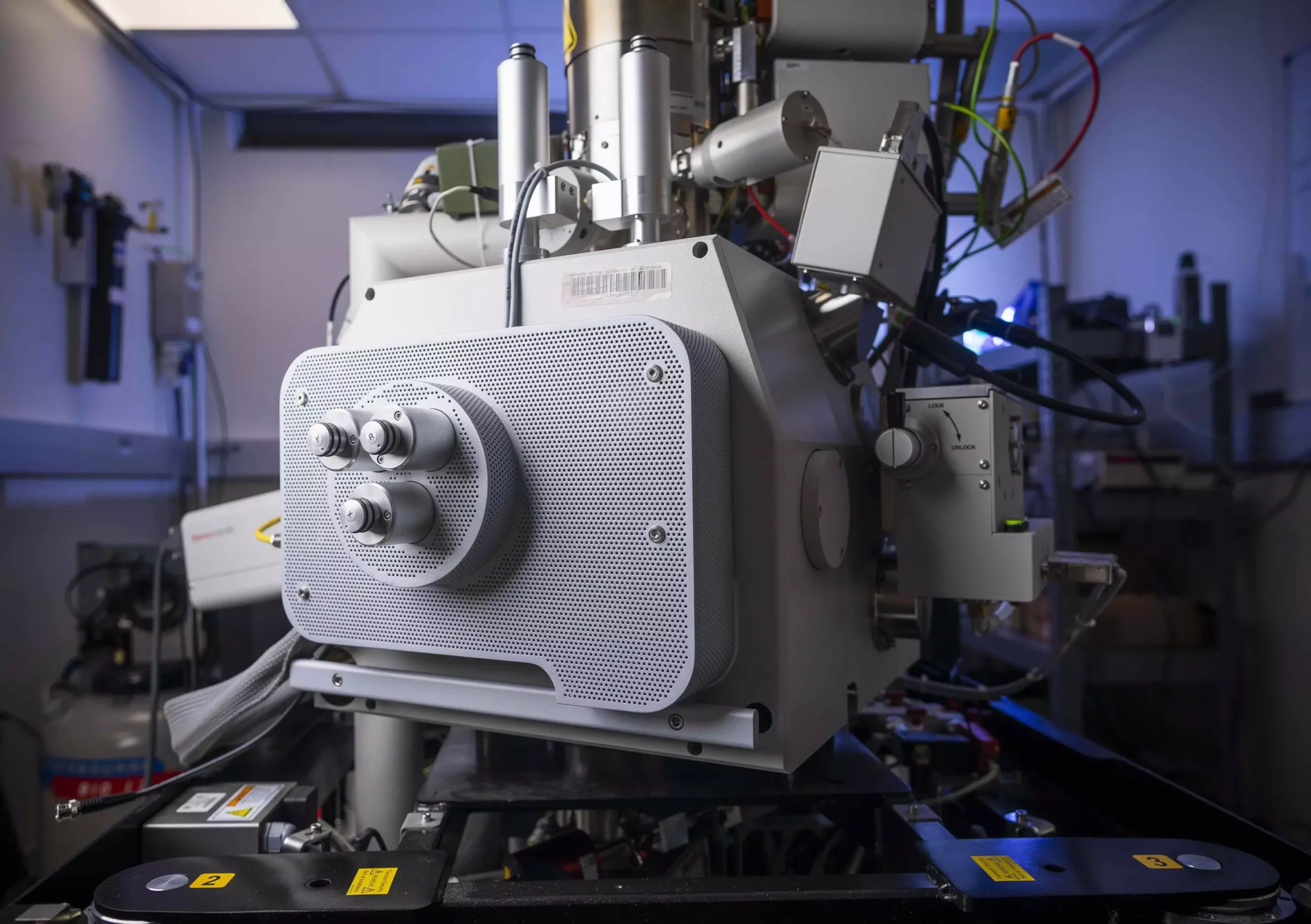
Utilizing advanced scanning ultrafast electron microscopy (SUEM), the research team has pioneered a method to visualize the movement of hot photocarriers in real time. Incorporating ultrafast laser pulses, the imaging technique essentially functions as a time-resolved “shutter,” allowing researchers to capture images of charge transfers that occur within a picosecond to nanosecond timeframe. By firing an electron beam to scan the interface between the excited materials, the team was able to create a real-time “movie” of the charge carriers in motion, offering a tangible glimpse into a phenomenon that was previously only theorized in textbooks.
The findings from this research elucidate the rapid migration of photocarriers in uniform regions of the silicon or germanium materials compared to their behavior at the heterojunction. While carriers that are generated within these uniform regions exhibit high speeds due to their initial high temperatures, those generated near the heterojunction face challenges. Here, a portion of the hot carriers can become trapped by the potential barrier at the junction, substantially impeding their movement and diminishing the overall mobility of the charge carriers. This charge trapping phenomenon, while understood theoretically, has now been corroborated by direct experimental observations, offering semiconductor device designers critical insights into optimizing performance.
The research conducted at UC Santa Barbara symbolizes a significant advancement in the understanding of semiconductor materials, particularly in relation to heterojunctions. The ability to visualize photocarrier dynamics opens new avenues for refining design strategies aimed at enhancing device performance and efficiency. This work not only honors the legacy of semiconductor thought leader Herb Kroemer, who championed the critical role of interfaces in device functionality, but it also propels the field toward innovative applications that align with the demands of modern technology.
As we continue to explore the intricate behavior of charge carriers in semiconductors, the implications of this research will resonate across various applications in electronics and renewable energy. By establishing a foundation for direct observation of phenomena that were once elusive, the team at UC Santa Barbara has paved the way for further advancements in semiconductor technology, ensuring that we remain on the cutting edge of electronic innovation. The journey of understanding and harnessing the power of hot photocarriers is just beginning, promising a future ripe with opportunities in energy efficiency and electronic performance.


Leave a Reply