
In a recent groundbreaking development, researchers at TMOS and RMIT University have introduced a new 2D quantum sensing chip utilizing hexagonal boron nitride (hBN). This innovative technology has the capability to detect temperature anomalies and magnetic fields in any direction, marking a significant advancement in the field of quantum sensing.
Limitations of Current Quantum Sensing Technology
Traditionally, quantum sensing chips have been constructed from diamond due to its robust nature. However, diamond-based sensors are limited in their ability to detect magnetic fields when not aligned with the field, resulting in large blind spots. This necessitates the use of multiple sensors with varying degrees of alignment, increasing operational complexity and limiting versatility in different applications. Moreover, the rigid and three-dimensional structure of diamond sensors restricts their ability to closely approach samples that are not perfectly smooth.
The Promise of hBN in Quantum Sensing
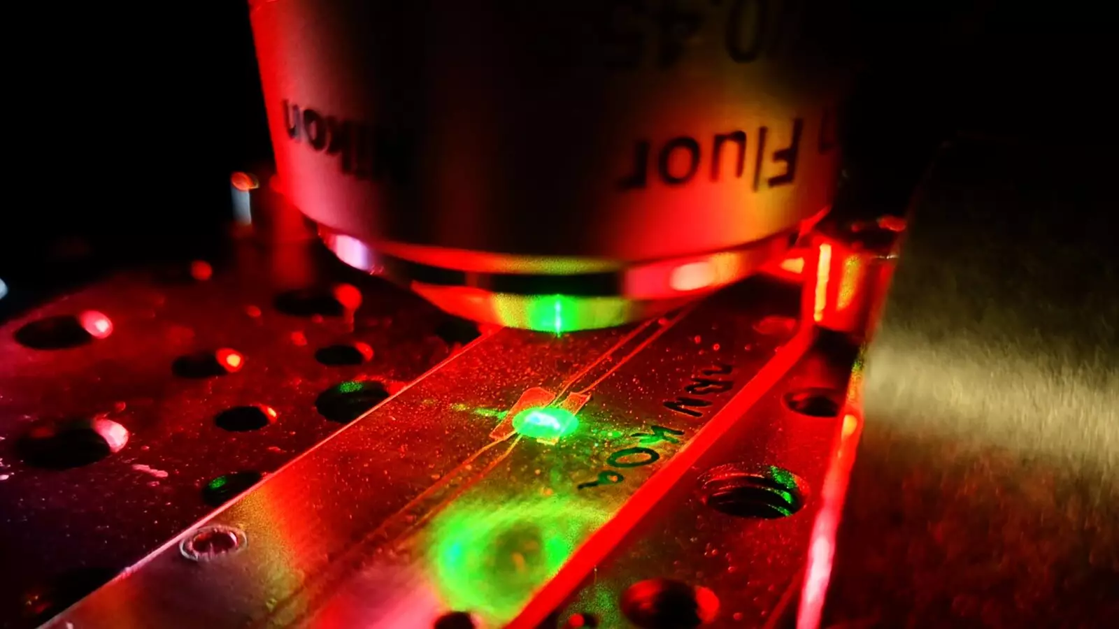
TMOS researchers led by Associate Investigator Jean-Philippe Tetienne and Chief Investigator Igor Aharonovich are pioneering a new quantum sensing platform using hBN crystals. These atomically thin sheets of hBN offer flexibility, enabling the sensing chips to conform to the shape of the sample under study and get closer to the sample surface compared to diamond-based sensors.
Uncovering a New Carbon-Based Defect
One of the key breakthroughs in this research is the discovery of a carbon-based defect in hBN that exhibits half spin behavior, allowing for the detection of magnetic fields in any direction. Through meticulous experimentation and comparison with known defects such as the boron vacancy defect, researchers were able to characterize the unique properties of this defect. This newfound defect opens up possibilities for controlling the sensor through electrical excitation and interacting with other defects within the same system.
The development of hBN-based quantum sensing chips holds significant promise for a wide range of applications. The isotropic nature of the carbon defect enables the simultaneous measurement of magnetic fields and temperature, paving the way for innovative sensing technologies. Furthermore, the 2D form factor of hBN allows for closer proximity to samples, enhancing the precision and accuracy of measurements.
Advantages of hBN Over Diamond
In comparison to diamond, hBN offers several advantages as a platform for quantum sensing. Its ultra-thin form factor eliminates the need for cryogenic cooling, making it suitable for room temperature quantum operations. Additionally, hBN is more cost-effective and readily accessible, making it a favorable choice for a wide range of applications.
Looking ahead, researchers are focused on identifying and understanding the atomic defects present in hBN to optimize sensor performance. By delving deeper into the composition of hBN, they aim to develop sensor devices that exhibit optimal efficiency and sensitivity. The potential applications of this technology span from magnetic geology exploration to radio spectroscopy, showcasing the diverse range of possibilities offered by this groundbreaking research.
Overall, the integration of 2D quantum chip technology using hBN represents a significant leap forward in the field of quantum sensing, offering enhanced capabilities and versatility for a wide array of applications. The future holds immense potential for further exploration and innovation in this burgeoning field, as researchers continue to push the boundaries of what is possible with quantum technology.
Leave a Reply