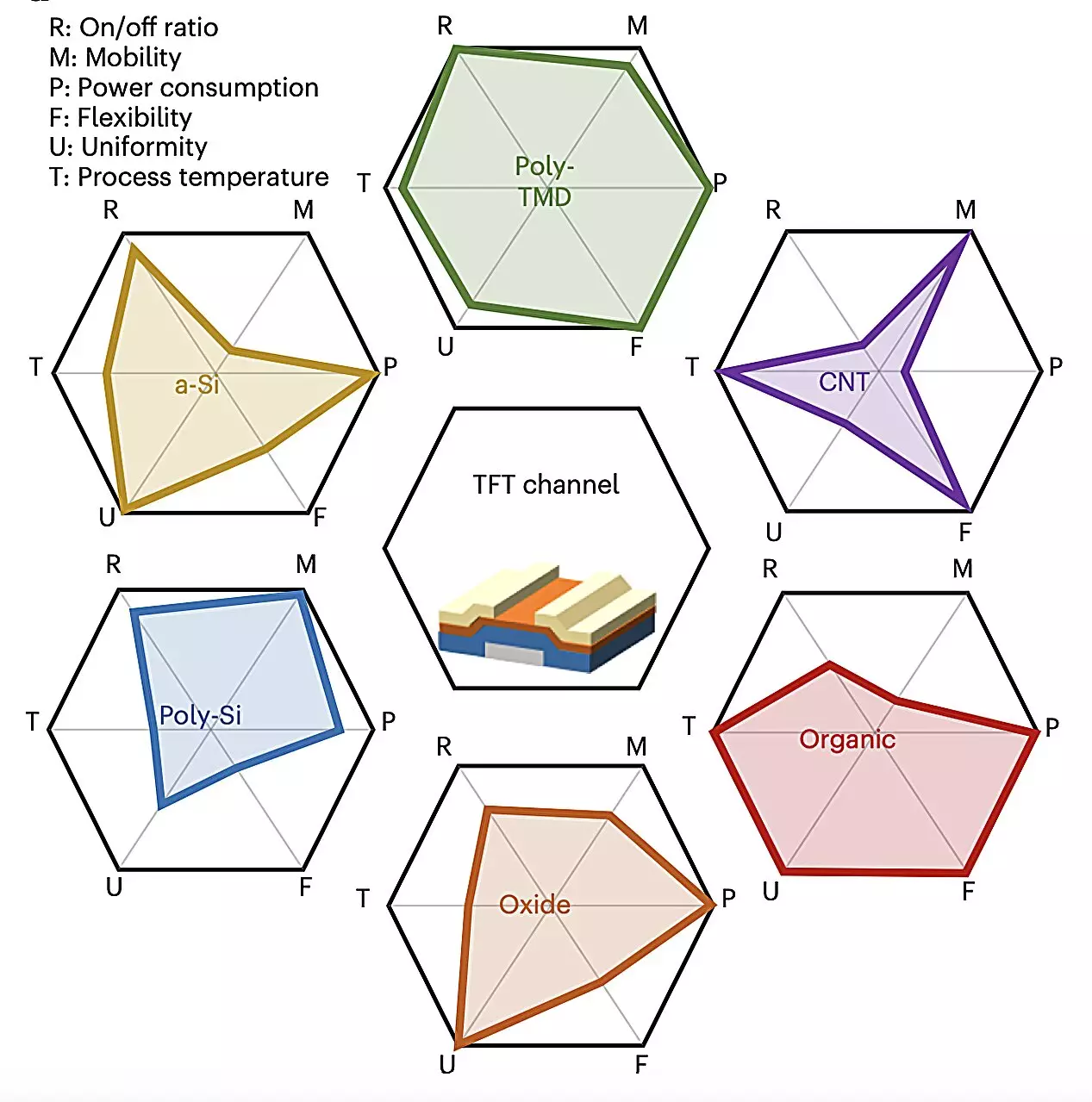
The field of electronics engineering has been witnessing a significant shift towards the development of ultra-small transistors in recent years. With the conventional silicon-based field effect transistors reaching their limitations in terms of scalability, researchers have turned their attention to alternative materials with higher electron mobility. Transition metal dichalcogenides (TMDs) have emerged as a promising candidate for the creation of scalable FETs, owing to their compact size and excellent carrier mobility characteristics.
Molybdenum disulfide (MoS2), a compound composed of molybdenum and sulfide atoms in a 1:2 ratio, has garnered attention from experts in the field. A team of researchers from Samsung Advanced Institute of Technology (SAIT) and Seoul National University recently showcased the successful integration of MoS2 transistors on a 200 mm wafer, marking a significant milestone in transistor technology. The study, published in Nature Electronics, underlines the potential of MoS2-based transistors in the future development of compact and versatile electronic devices.
According to Junyoung Kwon, Minsu Seol, and their collaborators, two-dimensional semiconductors like MoS2 offer unique advantages for thin-film transistor production, including scalability, transferability, atomic thinness, and high carrier mobility. While single-device demonstrations have shown promising results with single-crystalline two-dimensional films, the challenge lies in replicating this performance on a large scale using industrial methods. The successful integration of polycrystalline MoS2 field-effect transistors on a 200-mm wafer signifies a significant step forward in bridging this performance gap.
The research team employed metal-organic chemical vapor deposition (MOCVD) to fabricate large-scale arrays of MoS2 FETs, with a focus on eliminating the Schottky barrier at the MoS2 material-metal interface. By redesigning the fabrication process to address this issue, the team achieved a remarkable carrier mobility for the FETs, comparable to that of single-crystalline variations. Notably, the fabrication strategy adopted by the researchers aligns with existing electronic manufacturing processes, ensuring compatibility and a high yield rate exceeding 99.9%.
In initial tests, the MoS2-based FETs developed by the team showcased exceptional performance metrics, outperforming previous iterations in terms of field-effect mobility, contact resistance, and on-current densities. The team attributes this success to the innovative fabrication steps introduced, which not only improved the device performance but also paved the way for reducing contact resistance and enhancing carrier mobility. Additionally, the researchers identified key factors contributing to the enhanced device performance and uniformity on a 200 mm wafer, emphasizing the feasibility of large-scale fabrication in existing industrial settings.
Future Implications
By demonstrating the potential and viability of MoS2 integration in transistor technology, the research conducted by this team sets a precedent for future exploration and innovation in the field. The successful fabrication of highly performing MoS2-based FETs opens up avenues for developing advanced electronic devices with improved efficiency and scalability. As the quest for smaller, more efficient transistors continues, the findings of this study could serve as a catalyst for further research and development in the realm of semiconductor technology.


Leave a Reply